What Are Chiplets and Why They Are So Important for the Future of Processors
While chiplets have been in use for decades, they've been employed sparingly and for very specific purposes. Now, they're at the cutting edge of technology, with millions of people worldwide using them in desktop PCs, workstations, and servers.
An industry leader recently leveraged chiplets to regain its position at the forefront of innovation and it's clear that it won't be long before chiplets become the standard in the computing world. So, sit back and learn about chiplets and exactly why they are so important.
TL;DR: What are chiplets?
Chiplets are segmented processors. Instead of consolidating every part into a single chip (known as a monolithic approach), specific sections are manufactured as separate chips. These individual chips are then mounted together into a single package using a complex connection system.
This arrangement allows the parts that can benefit from the latest fabrication methods to be shrunk in size, improving the efficiency of the process and allowing them to fit in more components.
The parts of the chip that can't be significantly reduced or don't require reduction can be produced using older and more economical methods.
While the process of manufacturing such processors is complex, the overall cost is typically lower. Furthermore, it offers processor companies a more manageable pathway to expand their product range.
Silicon science
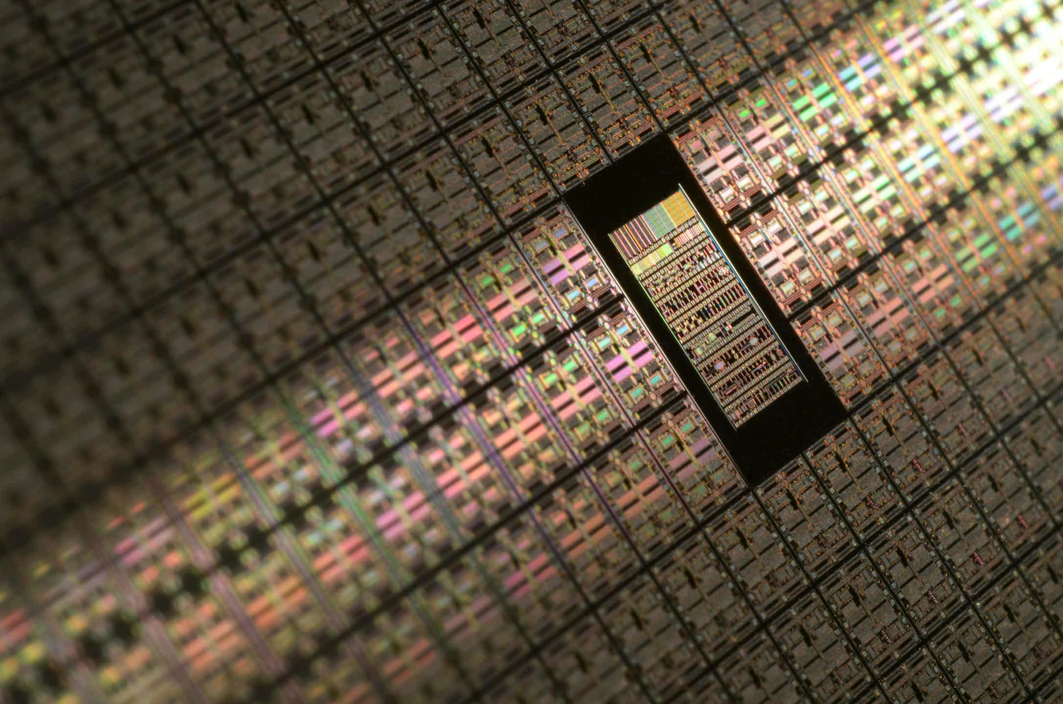
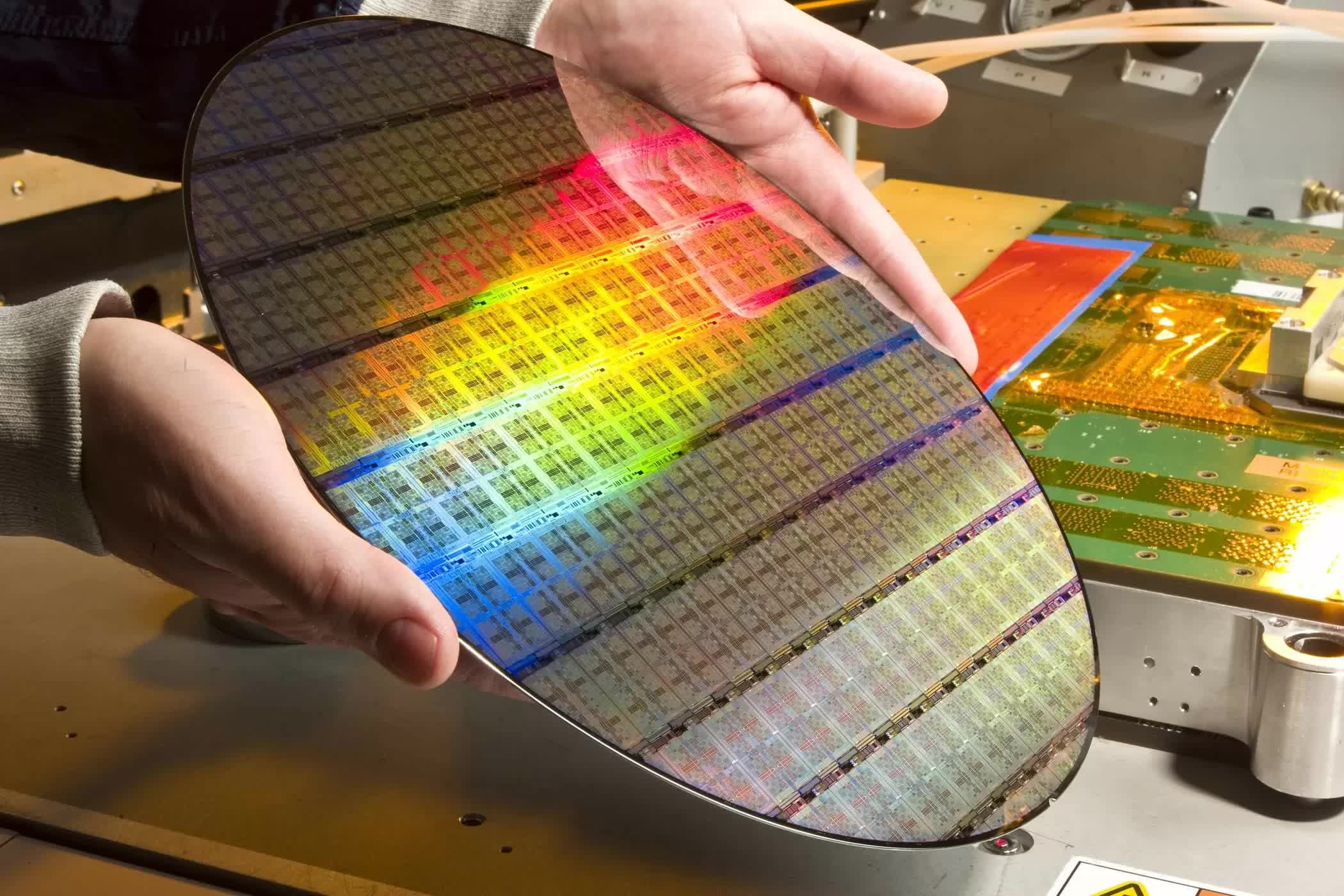
To fully understand why processor manufacturers have turned to chiplets, we must first delve into how these devices are made. CPUs and GPUs start their life as large discs made of ultra-pure silicon, typically a little under 12 inches (300 mm) in diameter and 0.04 inches (1 mm) thick.
This silicon wafer undergoes a sequence of intricate steps, resulting in multiple layers of different materials – insulators, dielectrics, and metals. These layers' patterns are created through a process called photolithography, where ultraviolet light is shone through an enlarged version of the pattern (a mask), and subsequently shrunk via lenses to the required size.
The pattern gets repeated, at set intervals, across the surface of the wafer and each of these will ultimately become a processor. Since chips are rectangular and wafers are circular, the patterns must overlap the disc's perimeter. These overlapping parts are ultimately discarded as they are non-functional.
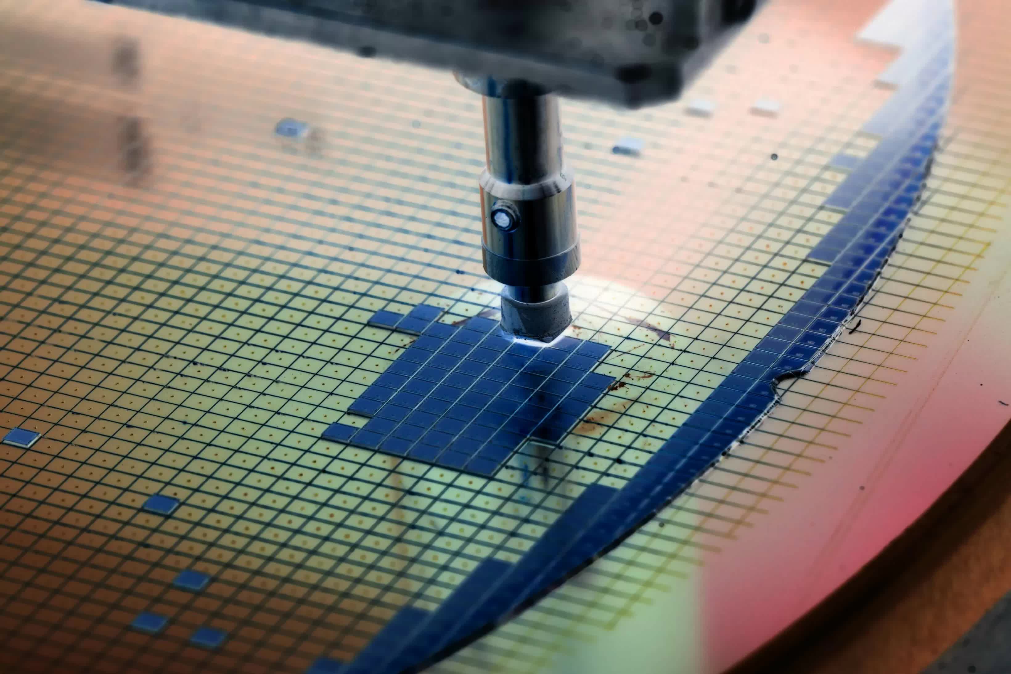
Once completed, the wafer is tested using a probe applied to each chip. The electrical examination results inform engineers about the processor's quality against a long list of criteria. This initial stage, known as chip binning, helps determine the processor's "grade."
For instance, if the chip is intended to be a CPU, every part should function correctly, operating within a set range of clock speeds at a specific voltage. Each wafer section is then categorized based on these test results.
Upon completion, the wafer is cut into individual pieces, or "dies," that are viable for use. These dies are then mounted onto a substrate, akin to a specialized motherboard. The processor undergoes further packaging (for instance, with a heat spreader) before it's ready for distribution.
The entire sequence can take weeks of manufacturing and companies such as TSMC and Samsung charge high fees for each wafer, anywhere between $3,000 and $20,000 depending on the process node being used.
"Process node" is the term used to describe the entire fabrication system. Historically, they were named after the transistor's gate length. However, as manufacturing technology improved and allowed for ever-smaller components, the nomenclature no longer followed any physical aspect of the die and now it's simply a marketing tool.
Nevertheless, each new process node brings benefits over its predecessor. It might be cheaper to produce, consume less power at the same clock speed (or vice versa), or have a higher density. The latter metric measures how many components can fit within a given die area. In the graph below, you can see how this has evolved over the years for GPUs (the largest and most complex chips you'll find in a PC)...
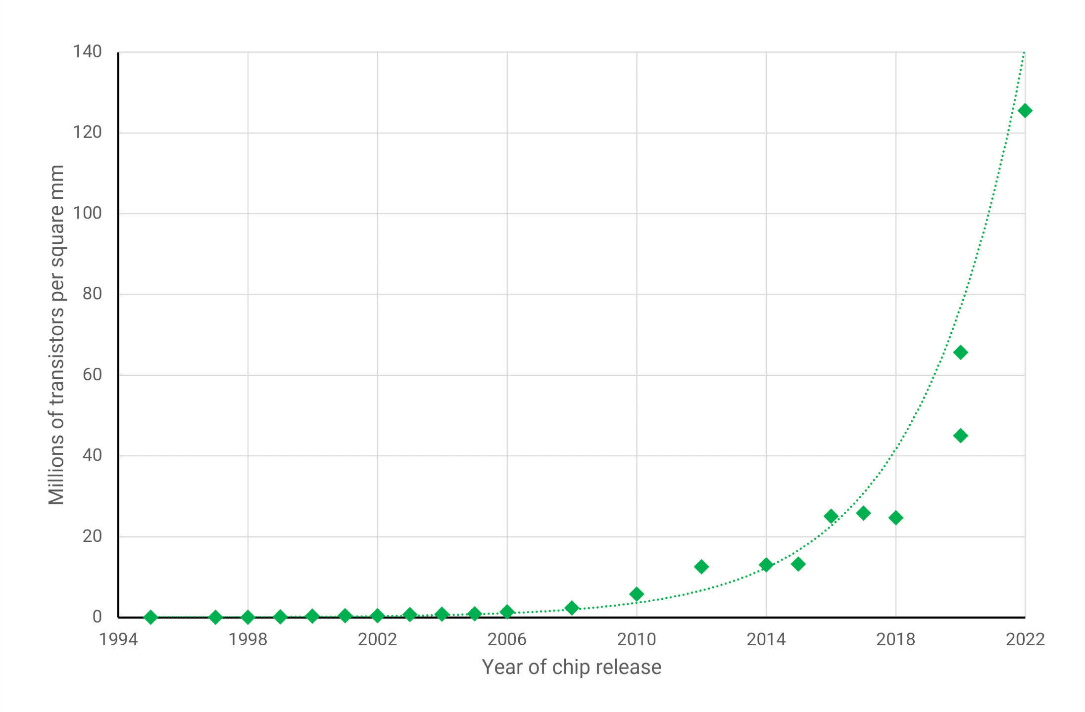
The improvements in process nodes provide a means for engineers to increase the capabilities and performance of their products, without having to use big and costly chips. However, the above graph only tells part of the story, as not every aspect of a processor can benefit from these advancements.
Circuits inside chips can be allocated into one of the following broad categories:
- Logic – handles data, math, and decision-making
- Memory – usually SRAM, which stores data for the logic
- Analog – circuits that manage signals between the chip and other devices
Unfortunately, while logic circuits continue to shrink with every major step forward in process node technology, analog circuits have barely changed and SRAM is starting to reach a limit too.
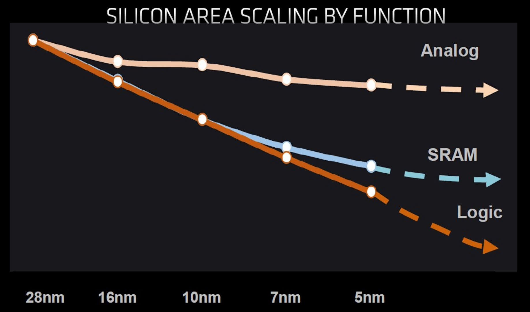
While logic still forms the largest portion of the die, the amount of SRAM in today's CPUs and GPUs has significantly grown in recent years. For example, AMD's Vega 20 chip used in its Radeon VII graphics card has a combined total of 5 MB of L1 and L2 cache. Just two GPU generations later, the Navi 21 has over 130 MB of assorted cache – a remarkable 25 times more than Vega 20.
We can expect these levels to continue to increase as new generations of processors are developed, but with memory not scaling down as well as the logic, it will become increasingly less cost-effective to manufacture all of the circuitry on the same process node.
In an ideal world, one would design a die where analog sections are fabricated on the largest and cheapest node, SRAM parts on a much smaller one, and logic reserved for the absolute cutting-edge technology. Unfortunately, this is not practically achievable. However, there exists an alternative approach.
Divide and conquer
Back in 1995, Intel launched a successor to its original P5 processor, the Pentium II. What set it apart from the usual fare at that time, was that beneath the plastic shield sat a circuit board housing two chips: the main chip, containing all the processing logic and analog systems, and one or two separate SRAM modules serving as Level 2 cache.
Intel manufactured the primary chip, but the cache was sourced from other firms. This would become fairly standard for desktop PCs in the mid-to-late 1990s, until semiconductor fabrication techniques improved to the point where logic, memory, and analog could all be integrated into the same die.
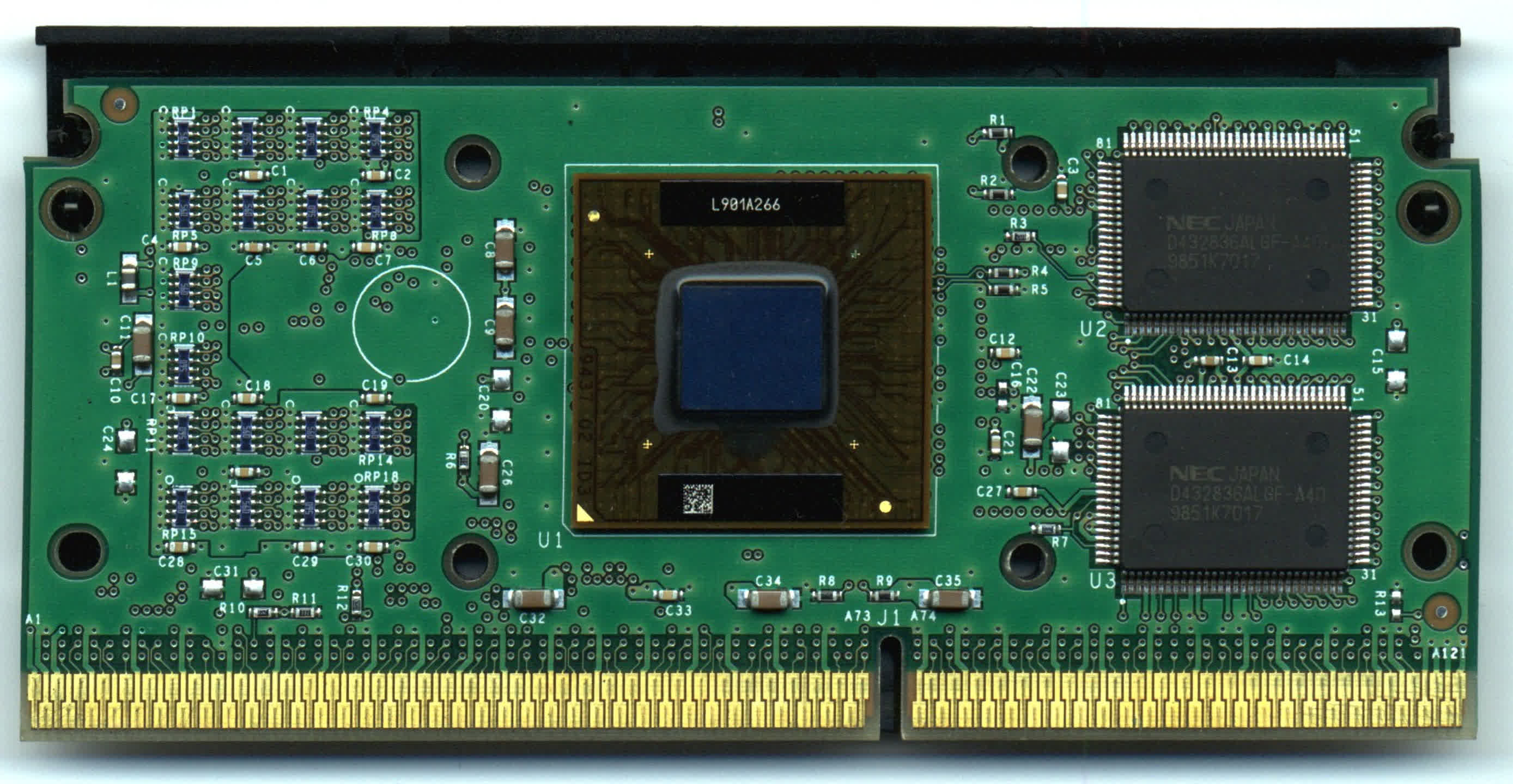
Intel's Pentium II – CPU in the middle, cache chips on the right. Source: Wikimedia
While Intel continued to dabble with multiple chips in the same package, it largely stuck with the so-called monolithicapproach for processors – i.e., one chip for everything. For most processors, there was no need for more than one die, as manufacturing techniques were proficient (and affordable) enough to keep it straightforward.
However, other companies were more interested in following a multi-chip approach, most notably IBM. In 2004, it was possible to purchase an 8-chip version of the POWER4 server CPU that comprised four processors and four cache modules, all mounted within the same body (known as a multi-chip moduleor MCM approach).
Around this time, the term "heterogeneous integration"(HI) started to appear, partially due to research work done by DARPA (Defense Advanced Research Project Agency). HI aims to separate the various sections of a processing system, fabricate them individually on nodes best suited for each, and then combine them into the same package.
Today, this is better known as system-in-package(SiP) and has been the standard method for equipping smartwatches with chips from their inception. For example, the Series 1 Apple Watch houses a CPU, some DRAM and NAND Flash, multiple controllers, and other components within a single structure.
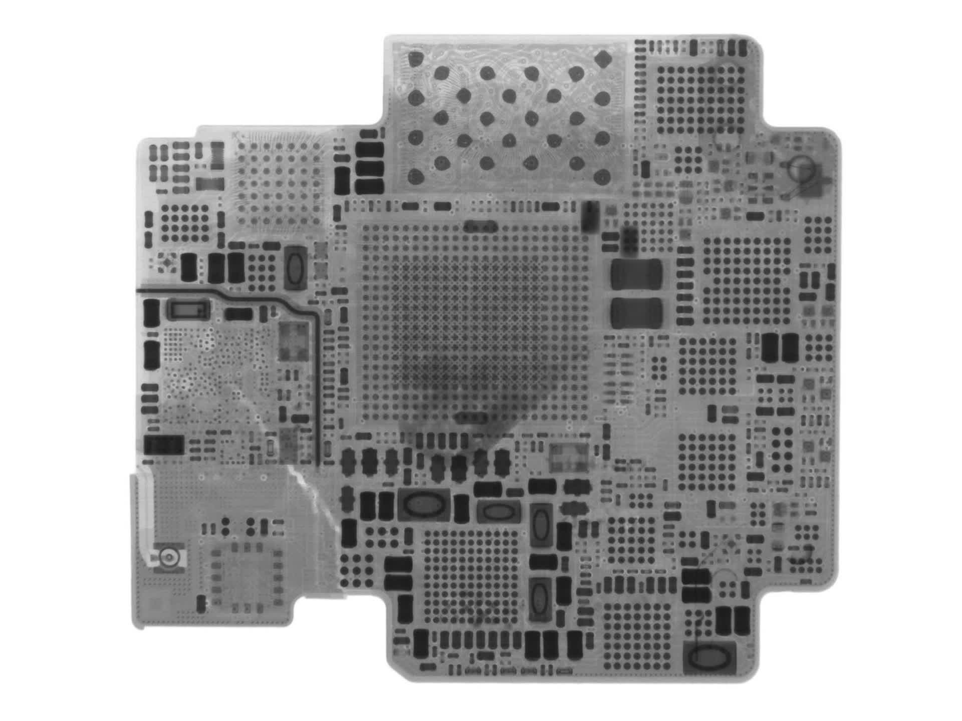
An x-ray of Apple's S1 SiP. Source: iFixit
A similar setup can be achieved by having different systems all on a single die (known as system-on-chipor SoC). However, this approach doesn't allow for taking advantage of different node prices, nor can every component be manufactured this way.
For a technology vendor, using heterogeneous integration for a niche product is one thing, but employing it for the majority of their portfolio is another. This is precisely what AMD did with its range of processors. In 2017, the semiconductor giant released its Zen architecture in the form of the single-die Ryzen desktop CPU. Several months later, two multi-chip product lines, Threadripper and EPYC, debuted, with the latter boasting up to four dies.
With the launch of Zen 2 two years later, AMD fully embraced HI, MCM, SiP – call it what you will. They shifted the majority of the analog systems out of the processor and placed them into a separate die. These were manufactured on a simpler, cheaper process node, while a more advanced one was used for the remaining logic and cache.
And so, chiplets became the buzzword of choice.
Smaller is better
To understand exactly why AMD chose this direction, let's examine the image below. It showcases two CPUs from the Ryzen 5 series – the 2600 on the left, employing the so-called Zen+ architecture, and the Zen 2-powered 3600 on the right.
The heat spreaders on both models have been removed, and the photographs were taken using an infrared camera. The 2600's single die houses eight cores, though two of them are disabled for this particular model.
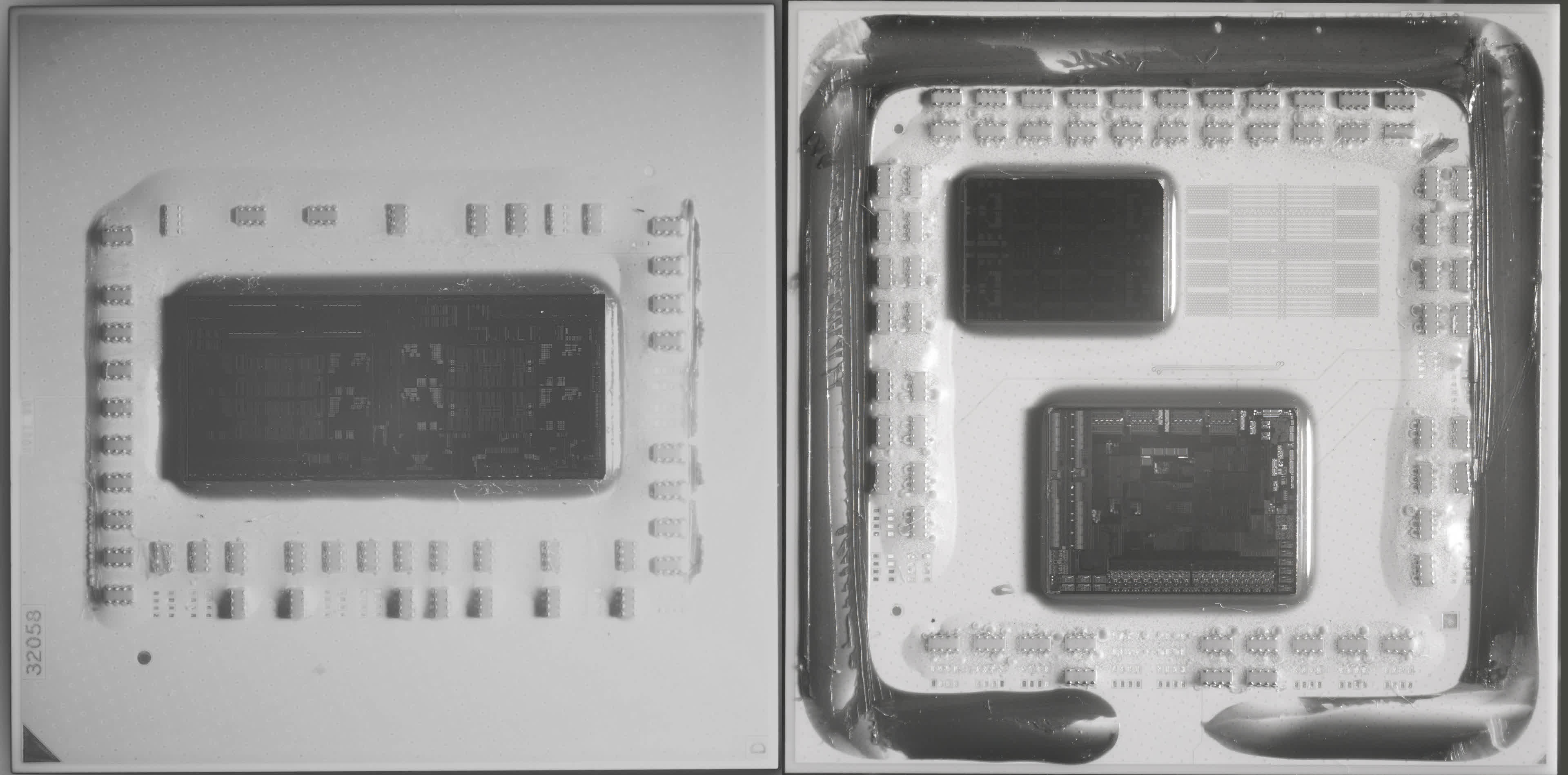
Source: Fritzchen Fritz
This is also the case for the 3600, but here we can see that there are two dies in the package – the Core Complex Die (CCD) at the top, housing the cores and cache, and the Input/Output Die (IOD) at the bottom containing all the controllers (for memory, PCI Express, USB, etc.) and physical interfaces.
Since both Ryzen CPUs fit into the same motherboard socket, the two images are essentially to scale. On the surface, it might seem that the two dies in the 3600 have a larger combined area than the single chip in the 2600, but appearances can be deceptive.
If we directly compare the chips containing the cores, it's clear how much space in the older model is taken up by analog circuitry – it's all the blue-green colors surrounding the gold-colored cores and cache. However, in the Zen 2 CCD, very little die area is dedicated to analog systems; it's almost entirely composed of logic and SRAM.
The Zen+ chip has an area of 213 mm² and was manufactured by GlobalFoundries using its 12nm process node. For Zen 2, AMD retained GlobalFoundries' services for the 125 mm² IOD but utilized TSMC's superior N7 node for the 73 mm² CCD.
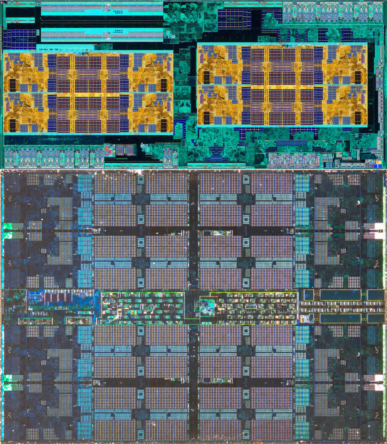
Zen+ (top) vs Zen 2 CCD (bottom)
The combined area of the chips in the newer model is smaller, and it also boasts twice as much L3 cache, supporting faster memory and PCI Express. The best part of the chiplet approach, however, was that the compact size of the CCD made it possible for AMD to fit another one into the package. This development gave birth to the Ryzen 9 series, offering 12 and 16-core models for desktop PCs.
Even better, by using two smaller chips instead of one large one, each wafer can potentially yield more dies. In the case of the Zen 2 CCD, a single 12-inch (300 mm) wafer can produce up to 85% more dies than for the Zen+ model.
The smaller the slice one takes out of a wafer, the less likely one is going to find manufacturing defects (as they tend to be randomly distributed across the disc), so taking all of this into account, the chiplet approach not only gave AMD the ability to expand its portfolio, it did so far more cost-effectively – the same CCDs can be used in multiple models and each wafer produces hundreds of them!
The smaller the piece taken from a wafer, the less likely one is to encounter manufacturing defects (since they tend to be randomly distributed across the disc). So, taking all of this into account, the chiplet approach not only enabled AMD to expand its portfolio, but it also did so much more cost-effectively. The same CCDs can be used in multiple models, and each wafer produces hundreds of them!
But if this design choice is so advantageous, why isn't Intel doing it? Why aren't we seeing it being used in other processors, like GPUs?
Following the lead
To address the first question, Intel is indeed adopting the full chiplet route, and it's on track to do so with its next consumer CPU architecture, called Meteor Lake. Naturally, Intel's approach is somewhat unique, so let's explore how it differs from AMD's approach.
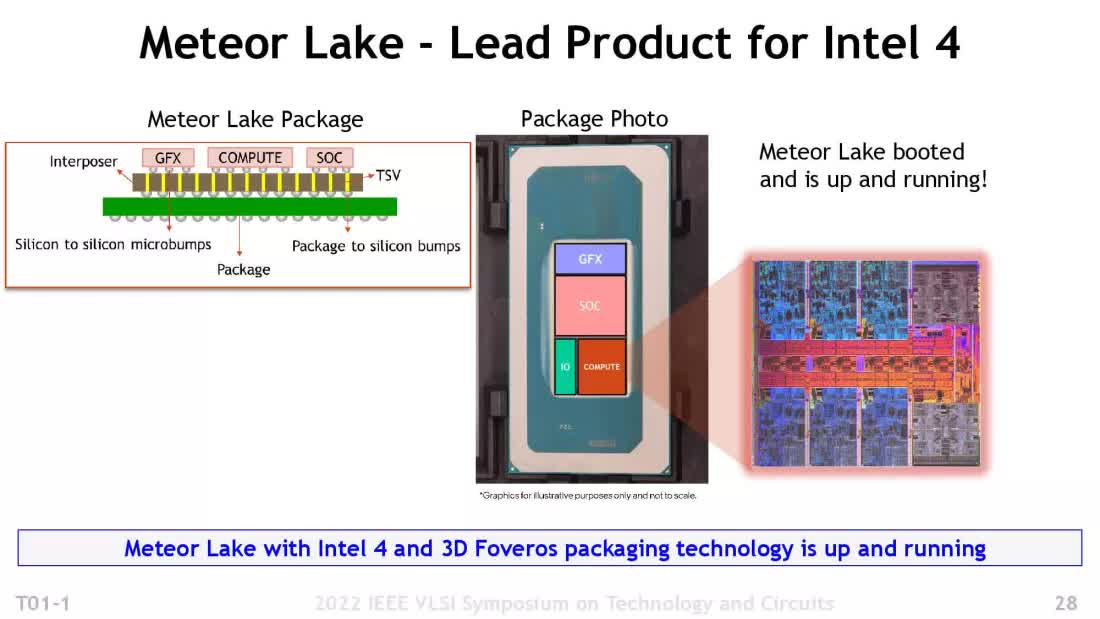
Using the term tilesinstead of chiplets, this generation of processors will split the previously monolithic design into four separate chips:
- Compute tile: Contains all of the cores and L2 cache
- GFX tile: Houses the integrated GPU
- SOC tile: Incorporates L3 cache, PCI Express, and other controllers
- IO tile: Accommodates the physical interfaces for memory and other devices
High-speed, low-latency connections are present between the SOC and the other three tiles, and all of them are connected to another die, known as an interposer. This interposer delivers power to each chip and contains the traces between them. The interposer and four tiles are then mounted onto an additional board to allow the whole assembly to be packaged.
Unlike Intel, AMD does not use any special mounting die but has its own unique connection system, known as Infinity Fabric, to handle chiplet data transactions. Power delivery runs through a fairly standard package, and AMD also uses fewer chiplets. So why is Intel's design as such?
One challenge with AMD's approach is that it's not very suitable for the ultra-mobile, low-power sector. This is why AMD still uses monolithic CPUs for that segment. Intel's design allows them to mix and match different tiles to fit a specific need. For example, budget models for affordable laptops can use much smaller tiles everywhere, while AMD only has one size chiplet for each purpose.
The downside to Intel's system is that it's complex and expensive to produce, although it's too early to predict how this will affect retail prices. Both CPU firms, however, are fully committed to the chiplet concept. Once every part of the manufacturing chain is engineered around it, costs should decrease.
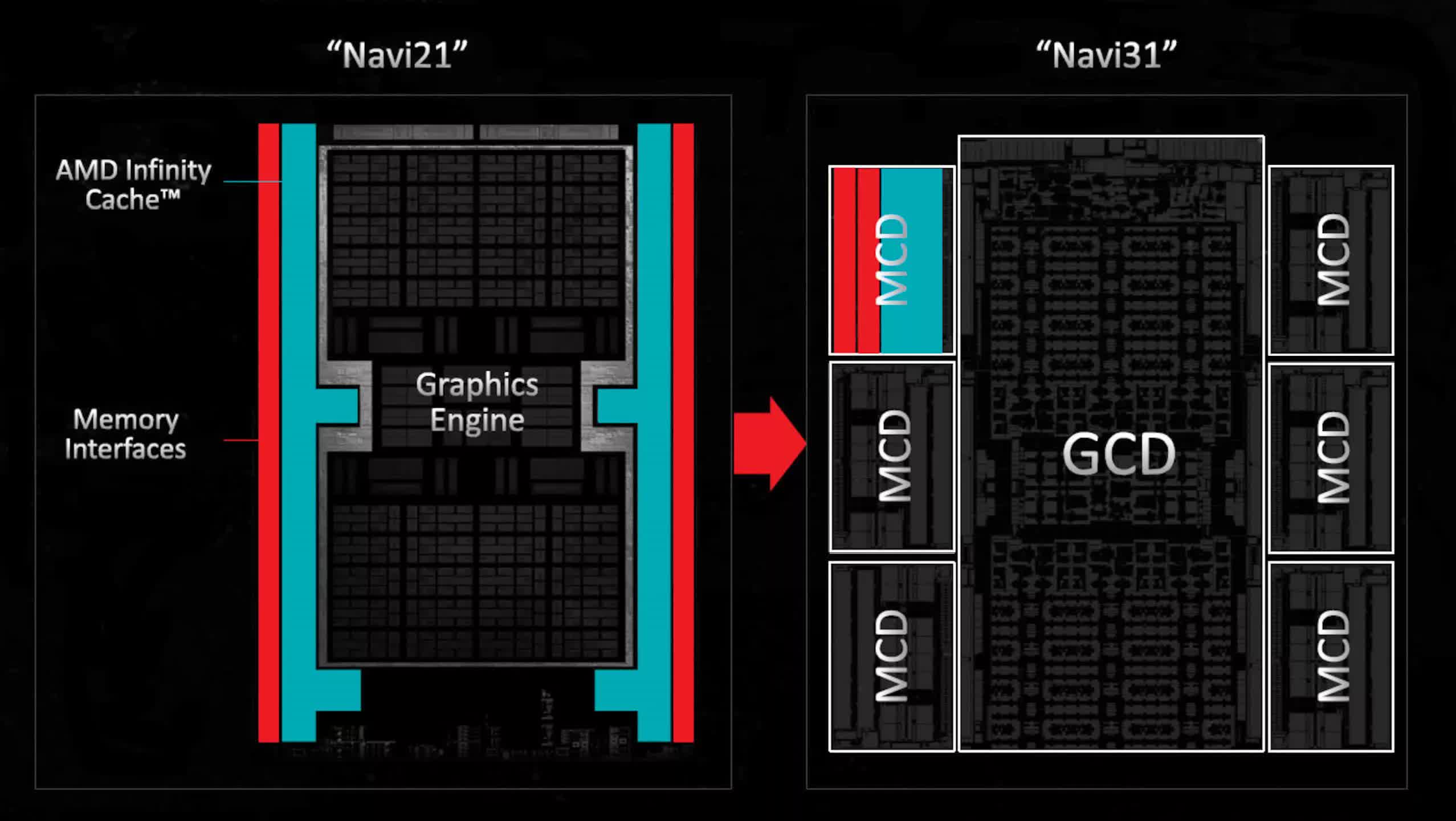
Regarding GPUs, they contain relatively little in terms of analog circuitry compared to the rest of the die, but the amount of SRAM inside is steadily increasing. This is why AMD applied its chiplet knowledge to its latest Radeon 7000 series, with the Radeon RX 7900 GPUs comprising multiple dies – a single large one for the cores and L2 cache, and five or six tiny chips, each containing a slice of L3 cache and a memory controller.
By moving these parts out of the main die, engineers were able to significantly increase the amount of logic without the need to use the very latest process nodes to keep chip sizes under control. However, the change didn't bolster the breadth of the graphics portfolio, although it probably did help improve overall costs.
Currently, Intel and Nvidia show no signs of following AMD's lead with their GPU designs. Both companies use TSMC for all manufacturing duties and seem content to produce extremely large chips, passing the cost onto consumers.
However, with revenues in the graphics sector steadily declining, we may see every GPU vendor adopting the same route within the next few years.
Getting Moore with chiplets
No matter whenthese changes occur, the fundamental truth is that they musthappen. Despite the tremendous technological advances in semiconductor manufacturing, there is a definite limit to how much each component can be shrunk.
To continue enhancing chip performance, engineers essentially have two avenues – add more logic, with the necessary memory to support it, and increase internal clock speeds. Regarding the latter, the average CPU hasn't significantly altered in this aspect for years. AMD's FX-9590 processor, from 2013, could reach 5 GHz in certain workloads, while the highest clock speed in its current models is 5.7 GHz (with the Ryzen 9 7950X).
Intel recently launched the Core i9-13900KS, capable of reaching 6 GHz under the right conditions, but most of its models have clock speeds similar to AMD's.
However, what haschanged is the amount of circuitry and SRAM. The aforementioned FX-9590 had 8 cores (and 8 threads) and 8 MB of L3 cache, whereas the 7950X3D boasts 16 cores, 32 threads, and 128 MB of L3 cache. Intel's CPUs have similarly expanded in terms of cores and SRAM.
Nvidia's first unified shader GPU, the G80 from 2006, consisted of 681 million transistors, 128 cores, and 96 kB of L2 cache in a chip measuring 484 mm2 in area. Fast forward to 2022, when the AD102 was launched, and it now comprises 76.3 billion transistors, 18,432 cores, and 98,304 kB of L2 cache within 608 mm2 of die area.
In 1965, Fairchild Semiconductor co-founder Gordon Moore observed that in the early years of chip manufacturing, the density of components inside a die was doubling each year for a fixed minimum production cost. This observation became known as Moore's Law and was later interpreted to mean "the number of transistors in a chip doubles every two years", based on manufacturing trends.
Moore's Law has remained a reasonably accurate depiction of the semiconductor industry's progression for nearly six decades. The tremendous gains in logic and memory in both CPUs and GPUs have been achieved through continuous improvements in process nodes, with components becoming increasingly smaller over the years.
However, this trend can't continue forever, regardless of what new technology comes about.
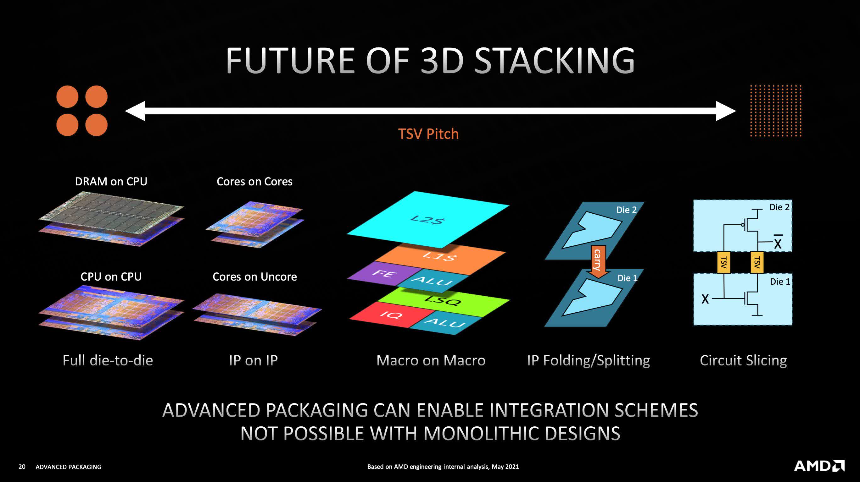
Instead of waiting for this limit to be reached, companies like AMD and Intel have turned to chiplets, exploring various ways they can be combined to continue progress in creating ever more powerful processors.
Decades in the future, the average PC might be home to CPUs and GPUs the size of your hand, but peel off the heat spreader and you'll find a host of tiny chips – not three or four, but dozens of them, all ingeniously tiled and stacked together.
The dominance of the chiplet has only just begun.
Keep Reading. Explainers at TechSpot
- Why Are Modern PC Games Using So Much VRAM?
- Deep Dive: AMD RDNA 3, Intel Arc Alchemist and Nvidia Ada Lovelace GPU Architecture
- Number Representations in Computer Hardware, Explained
- The Inner Workings of PCI Express
本文地址:http://www.signalforexgratis.com/column/63/
版权声明
本文仅代表作者观点,不代表本站立场。
本文系作者授权发表,未经许可,不得转载。